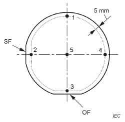
Figure 1 – Wafer sketch and measurement points
Figure 1 – Wafer sketch and measurement points 561-fig25-en.png