| Definition: | difference between the maximum thickness d1 and the minimum thickness d2 of a wafer as shown in Figure 1
X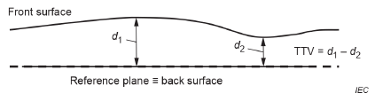
Figure 1 – Schematic diagram of a TTV
Note 1 to entry: Measurement of TTV is performed on a clamped wafer with the reference plane as defined in IEV 561-07-27, Note 1 to entry, item 1.
|